Research
ALD process development
With the semiconductor industry’s accelerating move towards building complex nanostructures in 3D (Vertical NAND flash memory, Nanosheet GAA transistors), the demand for conformal deposition on high aspect ratio structures has sky-rocketed. In addition, critical dimension (CD) control is becoming more and more challenging as device shrinks to the atomic scale. Atomic layer deposition (ALD), with its capability of atomic level control and theoretically perfect conformality, is perhaps the only existing deposition technology capable of meeting all these new challenges.
Active work at Applied Materials (2024-Present):
- Develop plasma based treatment for MEOL logic applications.
- Develop low temperature selective metal films for MEOL logic applications.
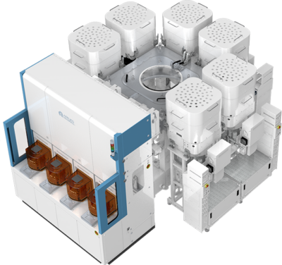
Publicly available image of Centris® platform is shown on the right.
Work done at ASM (2021-2024):
- Develop conformal (structure aspect ratio > 1000:1), low resistivity, fluorine free, minimal stress metal ALD films for Vertical NAND flash memory applications.
- Develop low temperature selective metal ALD films for BEOL logic applications.
- Explore various process strategies and CIP hardware to enable the above at HVM.
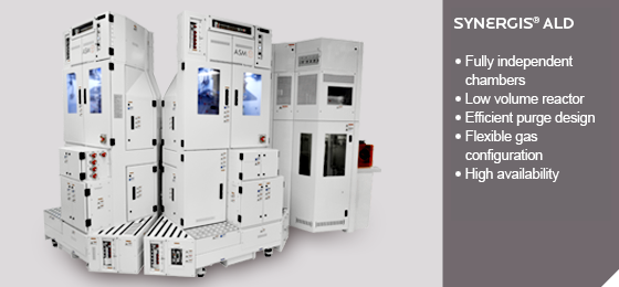
Publicly available image of Synergis® ALD platform is shown on the right.
Work done at Applied Materials (2019-2021):
- Optimize existing Plasma-enhanced Atomic Layer Deposition (PEALD) processes by understanding key reaction mechanisms in the associated plasma chemistry.
- Develop new precursors and identify new ALD pathways that enable novel dielectric films for FEOL logic applications.
- Explore self-limiting activation/passivation processes for substrate selective ALD.
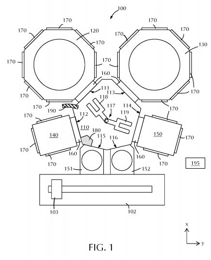
Publicly available patent diagrams on Olympia® system configurations are shown on the right.
